 Support l'X
 A new experimental approach to investigate defects in semiconductors
Like all crystalline materials, semiconductors are made up of atoms arranged in a perfectly regular pattern in space. But real materials are never perfect. Even when they are produced on an industrial scale using state-of-the-art processes, semiconductors still have defects. These alter the local electronic structure of the material, which can have negative consequences, but can also be beneficial for applications. This is why it is so important to understand the fundamental physics behind them. This is what a team at PMC has just done, thanks to the work carried out by Agatha Ulibarri during her thesis and published in the journal Physical Review Letters.
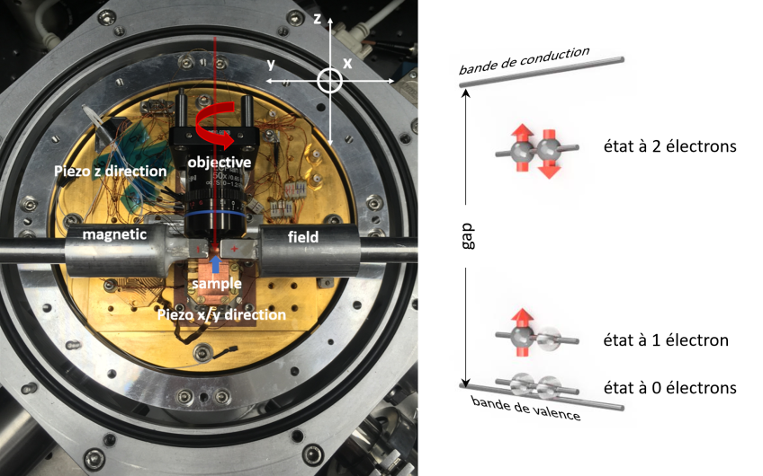
The semiconductor in question here is an alloy of gallium, arsenic and nitrogen (GaAsN). Occasionally, a gallium atom does not follow the usual regular arrangement, and instead lodges itself between other atoms. This “interstitial” defect alters the energy levels that the material's electrons can occupy. In a semiconductor, electrons can circulate in energy bands: the valence band and, at higher energies, the conduction band. For example, an electron that gains sufficient energy can move from the valence band to the conduction band, and then “fall back” into the valence band, losing energy in the form of light. Between the two bands, there is a band of forbidden energy, known as the “gap”, in which, in theory, there are no energy levels available for electrons. The presence of defects leads to the appearance of electronic levels in the gap. Rather than falling straight back into the valence band, a conduction-band electron can then also recombine in two stages, via these gap levels. This two-step process emits no light.
Determining the energies of these levels is crucial,” stresses Alistair Rowe, a physicist at PMC. For example, if these levels are 'deep' in the bandgap, this can often be detrimental to devices designed with these semiconductors". In their scientific publication, the PMC researchers, in collaboration with their colleagues at the University of Melbourne in Australia, have for the first time characterized the energy of these states due to the presence of this type of interstitial defect in the GaAsN alloy. Above all, thanks to an original experimental method, they have succeeded in showing how this electronic structure depends on spin. Like electric charge, spin is an intrinsic property of electrons, which can take on only two values. With their pol-PICTS method using circularly polarized light, electrons moving from the valence band to the conduction band were predominantly of a given spin, enabling a detailed study of how recombination via gap states was spin-sensitive. The results show that there is not just one but three states induced by the presence of gallium interstitial defects in GaAsN. Their energies disagree with theoretical predictions.
"These values depend on the exact nature of the chemical environment around the defect, which is still poorly understood,” explains Alistair Rowe. Our data could provide theorists with a benchmark for unveiling this environment by comparing the results of their calculations with our experiments."
This work, which draws on the PMC's extensive expertise in semiconductor physics, provides a better understanding of the physics due to this interstitial defect, which could be put to good use in applications, as are other defects known as “NV centers” in diamond today. Finally, the pol-PICTS method could prove very useful for probing other materials.
*PMC: a joint research unit CNRS, École Polytechnique, Institut Polytechnique de Paris, 91120 Palaiseau, France
More information :
Deep-Level Structure of the Spin-Active Recombination Center in Dilute Nitrides
Agatha C. Ulibarri et al., Deep-Level Structure of the Spin-Active Recombination Center in Dilute Nitrides, Physical Review Letters (2024)
https://journals.aps.org/prl/abstract/10.1103/PhysRevLett.132.186402